Malvern Panalytical의 'AERIS FOR THIN FILMS: GRAZING INCIDENCE X-RAY DIFFRACTION'을 이용한 응용자료는 말번 파날리티칼 코리아에서 제공하였으며 주요 내용은 다음과 같다.
Introduction
Thin films as polycrystalline coatings are used in many different application areas ranging from biomedical coatings on medical implants to spray-coated paints on automotive steels, deposited films on electrodes in batteries or metallic contacts in semiconductors, optical coatings on displays, to name a few.
As new applications for thin films emerge and existing applications become mainstream, the technology of deposition is always advancing, and the materials deposited are always being improved.
The crystalline phases deposited and the residual stresses in deposited films are key parameters for assessing the efficacy of a deposition method or a processing step. Monitoring the integrity of a film during the use is also vital to ensuring the longterm success of a product. With Grazing Incidence X-Ray Diffraction(GIXRD) you can target your configuration to maximize the signal from your coating. This gives you the best possible data from which to obtain the results you need, whether you need detailed studies of crystalline phases or rapid high throughput quality control.
Here we provide some example data and analysis showing the performance of Aeris for studying polycrystalline coatings.
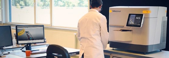
Figure 1: Enjoy a truly versatile powder diffraction capability in a compact state-of-the-art instrument.
Aeris configured for grazing incidence X-ray diffraction
With grazing incidence X-ray diffraction, you achieve a much-improved peak signal from thin films, where regular symmetric (Bragg-Brentano) powder scans may not yield sufficient peak intensity or give too much interference from the substrate.
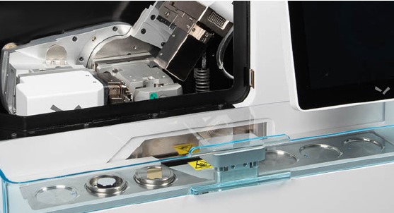
Aeris can be a dedicated thin film diffractometer for routine measurements or alternatively a versatile powder diffractometer enabling occasional thin film measurements. The high-performance de-coupled goniometer scanning technology provides highly reproducible 2θ scans at a range of precise incident beam(ω) angles suitable for grazing incidence X-ray diffraction(GIXRD) and residual stress measurements.
The parallel plate collimator on the diffracted beam side converts Aeris into the parallel beam measurement mode providing accurate peak positions and resolving defocusing effects, to bring you high quality data. A range of robust sample holders provides a variety of sample mounting options to suit your requirements.
Figure 2: Samples waiting in the Aeris loading area and an internal view of the Aeris in Grazing Incidence configuration. Solid sample holder on the left. Film holder on the right.
50nm thin film of polycrystalline Iridium on Silicon substrate
The refractory metal Iridium has many applications in high performance optical devices due to its high reflectivity of X-rays, low oxidation rate, and high melting point. For example, Iridium is researched as an alternative to gold and silver as an optical coating in high performance telescopes.
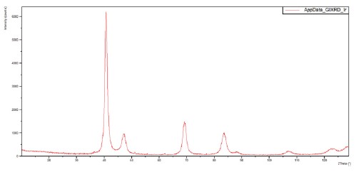
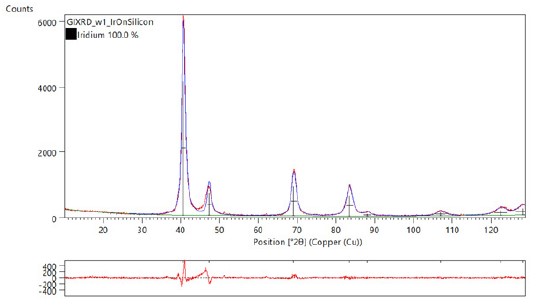
The crystallite size and micro-strain are good indicators of the film microstructure and overall quality of the film and can be quickly and non-destructively monitored by looking for changes in the diffraction peaks. For such a thin film, the Iridium diffraction peaks could easily be lost in the signal from the substrate peak. By using the grazing incidence diffraction geometry, it is possible to get clear and useful data quickly(See Figure 3.1).
The high angle peaks from the layer, such as the 85o peak, are only visible in the GIXRD scans as they are too weak to be seen in the reflection configuration.
Using HighScore analysis software [1], results for average crystallite size(11.1 nm), and micro-strain(0.585%) are quickly obtained(See Figure 3.2). These are structural parameters that help you to monitor and optimize your fabrication processes to obtain the required layer performance and product quality control.
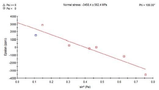
For thin films and coatings, it is important to measure residual stress in the film both to understand how the residual stress forms in the layer during deposition and to understand the final quality of the film. Thin films can support high stresses and, in addition to offering chemical protection to a component, coatings can provide additional strength to a component or conversely weaken the whole component.
Alternatively, a thin film that is overstressed can crack easily or become detached from the substrate. Crystallographic residual stress is a major quality control parameter in thin film processing. The residualstress within the layer can be determined using multiple-{hkl} residual stress analysis in Stress Plus [2] software (See Figure3.3).
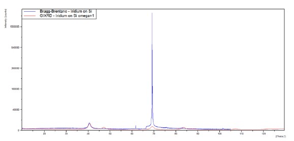
Comparison of the GIXRD data with conventional Bragg-Brentano data in Figure 3.4 shows that both Iridium and Silicon have strong diffraction peaks close to 69º 2θ. With a GIXRD scan the smaller Iridium peak is now clearly visible and not hidden by the Silicon substrate peak and the higher angle peaks such as at 85º and 107º are more easily seen.
Figure 3.1: GIXRD measurement of a polycrystalline Iridium layer on a Silicon single crystal substrate measured with the new Aeris thin film setup showing a very good data quality.
Figure 3.2: The data allow phase analysis including fitting as shown on this example exported from HighScore Plus best fit was obtained for crystallite size value 11.1nm and micro-strain value 0.585%.
Figure 3.3: The residual stress within the layer can be determined using multiple-{hkl} residual stress analysis in Stress Plus software.
Figure 3.4: Comparison of the GIXRD data with conventional Bragg-Brentano data clearly shows the benefit of the thin film analysis approach as it completely suppresses the intense substrate signal close to 69º and the higher angle peaks such as at 85º and 107º are more easily seen.
Pb-Br-Perovskite on glass substrate
The processing methods and properties of PbBr3NCH5 perovskite thin films are being researched as promising candidates for solar cells and detectors. They can be produced by a variety of deposition methods including cost-effective liquid coating.
It is always important to maintain control of the structure throughout any processing steps. The crystal structure, crystallite size and residual stress are all important parameters in determining both the optoelectronic efficiency and structural robustness of the material during use.
These layers are designed for optimum absorption of solar energy wavelengths and this means that they are quite transparent to X-rays. The grazing incidence configuration therefore maximizes the signal that can be obtained from the layers and so is the preferred geometry for the most efficient data collection.
Here we show examples of high-quality GIXRD data and analysis. The parallel beam optics with grazing incidence reduces beam broadening and hence leads to more accurate determination of crystallite size, strain, and residual stress. Grazing incidence geometry improves intensity from thinner films, where regular powder scans may not yield sufficient intensity for analysis.
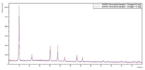
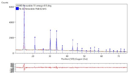
Figure 4.1 shows data collected at different angles of incidence (Omega). At omega 0.5º(Red scan) the signal to background of the layer peaks are better than with omega 1º(Blue scan).
Unlike the example in section 3, the substrate is glass which, being amorphous, provides a high background intensity. Being able to optimize the scan and reach low incident angles such as 0.5º is a great benefit for this kind of sample.
Crystal structure refinement is an important measurement for perovskites, even small changes in the crystal structure can have a large effect on the optical properties of this material.
Fig 4.2 shows a best fit for refinement of the Perovskite structure using HighScore Plus analysis suite. In this way, the crystal structure can be continuously understood, and the optical properties controlled.
Figure 4.1: GIXRD measurement of a thin polycrystalline Perovskite layer deposited on a glass substrate measured with the new Aeris thin film setup collected with 2 different angles of incidence. The data shows a very good quality and illustrates how angle of incidence can be optimised to obtain best quality GIXRD data.
Figure 4.2: The data enables good quality phase analysis including fitting and structure refinement as shown on this example exported from HighScore Plus.
Summary
With Aeris, you have all the capability of powder diffraction in one compact instrument. Here we have shown two examples of grazing incidence X-ray diffraction(GIXRD) which demonstrate the versatility of Aeris and the quality of data. With our patented and unique PreFIX optical mounting system, Aeris is easily reconfigured for quick comparison of data from Bragg Brentano, Transmission and GIXRD methods. GIXRD scans can be obtained within minutes and data at different angles of incidence can be compared to optimize the data collection settings.
Together with our analysis software HighScore Plus and Stress Plus, high quality data show the phase purity, crystallinity, crystallite size, micro-strain and residual stress for a complete view of your polycrystalline thin-film sample.
'AERIS FOR THIN FILMS: GRAZING INCIDENCE X-RAY DIFFRACTION'에 대한 궁금한 내용은 본 원고자료를 제공한 말번 파날리티칼 코리아를 통하여 확인할 수 있다.
Reference(참고문헌):
[1] The HighScore Suite, T. Degen, M. Sadki, E. Bron, U. KÖnig, and G. Nénert; Powder Diffr., Vol. 29, No. S2, December 2014
[2] Stress Analysis of polycrystalline thin films and surface regions by X-ray diffraction; U Welzel, J. Ligot, P. Lamparter, A.C. Vermeulen and E.J. Mittemeijer; J.Appl.Cryst.(2005).38, 1-29.
Model Name(모델명): Aeris
The Person in Charge(담당자): Hyunjung Gu
Maker(제조사): Malvern Panalytical
Country of Origin(원산지): Netherlands
Mail inquiry(기사문의): info.korea@malvern.com
Data Services(자료제공): Malvern Panalytical Korea
<이 기사는 사이언스21 매거진 2021년 5월호에 게재 되었습니다.>


 이전기사 :Purification of Vanillin by a Combination of Flash and Preparative HPLC with the PLC 2250
 다음기사 :Application Note·PlasmaQuant® PQ 9000 Elite